Inside the Nintendo Entertainment System (25th Anniversary)
October 15th, 2010 by Benj Edwards
In October 1985, Nintendo released the Nintendo Entertainment System (NES) in the United States. 25 years later, I took one apart for the wood-grained glory that is my “workbench series” of tech autopsies (this is my 11th entry). It’s up now on PC World.com.
Back in 2008, I dismantled the NES’s Japanese counterpart, the Nintendo Famicom (the NES’s Japanese counterpart), if you’re curious to see that. There’s a full list of my workbench teardowns below.
I hope you enjoy it. When you’re done, feel free to share your fondest NES memories in the comments below.
—
Here are my previous workbench teardowns: Atari 1040STf, Atari 800, Commodore Amiga 1000, Commodore 64, Nintendo Game Boy, Nintendo Famicom, Apple IIc, IBM Model M Keyboard, TRS-80 Model 100, and Macintosh Portable.


October 15th, 2010 at 8:42 pm
Ah, familiar territory. I’ve spent more time inside NES consoles than any other, (which sounds oddly suggestive now that I think about it…) in my efforts to combat the problems which plague the well-used toasters. One time I had to swap out a 72-pin connector twice in one afternoon order to calm the old grey box’s seizures.
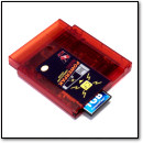
I also find it absurd how small the circuit board is in the NES carts. I would occasionally deep-clean my NES carts by opening them up, and the first time I did, it felt like I should be able to rent out all that extra space. I know they wanted to make them feel more like VHS tapes than video came carts at the time, but man was it overkill. Also amazed me at what debris could build up inside the carts over the years.
October 15th, 2010 at 9:36 pm
I always enjoy your teardowns. There are two points I am a little curious about, though.
First, in the controller, it seems to be lacking the chip that would go inside. Maybe it is on the other side of the board, though. The chip is an 8 bit shift register. Each button (notice that there are 8) would correspond to one bit in that register. When the game wanted to read it, it would start clocking one pin in the connector, and the shift register would put each bit on a data line. The NES would clock it 8 times each time it would read the controller. I only know this because I made use of a controller in a project.
The second thing I note is that I don’t believe every cartridge was so empty. I know that Gameboy’s had a variety of cartridge types.
October 15th, 2010 at 9:38 pm
Woops, hit submit too early. As I was saying,
I know that the Gameboy had a variety of cartridge types that would identify themselves differently. Some would have more ROM chips and have more data available. Some would have a bit of writable memory for saving. I would imagine that the NES was the same, where some cartridges would need more room for more ROM and for memory chips for saving.
October 16th, 2010 at 12:08 am
Nice photo essay. For anyone interested in a variety of NES cartridge PCBs (they came in all shapes and sizes and some came closer to filling the whole space provided), here are a bunch of boards I scanned:
http://multimedia.cx/nesgallery/
October 16th, 2010 at 12:12 am
Grrr… your picture of the NES cartridge PCB has the PRG and CHR labels reversed! Ah, like it matters. 🙂 (Just working off my own picture of the SMB ROM.)
October 16th, 2010 at 12:16 am
@jdiwnab: The shift register is on the other side of the controller PCB shown in slide 14. Yep, I’ve disassembled one before. 🙂
October 16th, 2010 at 7:12 am
Glad you like it, guys.
jdiwnab: Like Mike said, the IC for the Control Pad is on the other side of the board. Also, I’ve never seen a cartridge PC board (even battery-backed ones) take up more than half of its plastic case, which Mike’s link illustrates quite nicely.
Mike: Yep, it looks like I did flip the labels (doh!). I was probably looking at the board upside down to read the text on each chip but then forgot to flip it the other way in my head. I just submitted a corrected slide to my editor, which will hopefully make its way in place before the show is syndicated across the universe. 🙂
October 16th, 2010 at 10:28 am
@Benj: There seemed to be a lot of pirate or experimental/development carts that made use of more of the cartridge real estate. Check out:
SMB3 pirate hack: http://kevtris.org/mappers/single_pirates/BTL_MMC3A.html
VRC6 test cart: http://kevtris.org/nes/images/VRC6_TestCart.jpg
Mega Man 3 prototype: http://kevtris.org/nes/images/Megaman3_PCB.jpg
I think that website used to have a lot more interesting pictures that just weren’t correctly linked from the main page and are impossible to find now.
October 17th, 2010 at 2:28 pm
Great slideshow and commentary. You gave a great simple and clear look at the NES hardware. Well done!