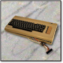
Mr. Wizard Explains the Atari 1200XL (Somewhat Badly)
June 29th, 2010 by Benj EdwardsYou remember Mr. Wizard’s World, right? It was a light science show for kids that aired on Nickelodeon in the 1980s. On one episode, Mr. Wizard took a peek inside the Atari 1200XL with his usual juvenile accompaniment. Here’s a clip.
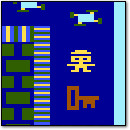
The real fun begins as Mr. Wizard tries to explain the function of a row of eight chips on the motherboard around 1:40 into the segment. He quickly lapses into apparent nonsense:
You see these eight all here? This is an eight bit computer. You’ve heard of that? OK. Each one of these sends a, uh, byte off to the screen and, uh, each little dot has to have a signal from each one of those.
I probably don’t have to tell you this, but that’s not how the Atari 1200XL works. This is Internet, though, so I’ll explain it. Those eight chips are RAM chips, and their exact quantity in any computer is mostly independent of the CPU’s word size (i.e. 8-bit, 16-bit).
The fact the Atari’s CPU is 8-bit and that it contains eight RAM chips is a coincidence that apparently confused Mr. Wizard. The 1200XL had 64KB of RAM, so those are likely 8KB chips (8KB x 8 chips = 64KB). To make up the same amount of RAM, Atari could have used (for example) four 16KB chips or sixteen 4KB chips.
The rest of his explanation for those eight chips doesn’t make any sense either. But hey, it’s Mr. Wizard! Other than that, he does a pretty good job showcasing the 1200XL in a kid-show context. The joystick-sans-stick demonstration is classic Mr. Wizard fare — he’d always change things around and make you think about an issue in an unexpected way. That was his genius.
I loved Mr. Wizard’s World dearly as a kid. In fact, I learned many basic physics principles from that show. We could really use someone like him again.
P.S. If you like Mr. Wizard as much as I do, watch him on The Late Show with David Letterman in 1982.


June 29th, 2010 at 11:15 pm
Apparently you haven’t seen “Bill Nye the Science Guy”. I’ve watched it a couple of times, and I have liked it.
June 30th, 2010 at 3:09 am
Actually, he’s not quite as wrong as he seems, though he is a bit confused. A lot of computers back then used RAM in which each chip was responsible for an eighth of each byte, each chip connected to a different line on the data bus. I’d bet those are 64kbit x 1 chips, not 8kbit x 8.
June 30th, 2010 at 7:34 am
Oh I’ve seen Bill Nye, all right, but he’s no Mr. Wizard.
June 30th, 2010 at 7:39 am
I second what Dezro has said, it would most likely be eight 64Kx1 chips. Mr.Wizard is not wrong, but he probably didn’t explain very well how RAM is really organized.
June 30th, 2010 at 8:01 am
I meant 8 kilobyte chips, not 8 kilobit chips. Sorry for the confusion. The 1200XL does in fact use “64×1” chips — but 64 kilobits is 8 kilobytes, so we’re talking about the same thing.
My main point is that the number of chips doesn’t necessarily have anything to do with it being an “8-bit” system. For example, the Atari XE Game System has 64KB of RAM and only uses two 64×4 chips (32KB a piece).
June 30th, 2010 at 8:24 am
It could very well be that in the day when this video was made, N x 1 was the only kind of DRAM available
June 30th, 2010 at 6:08 pm
Mr Wizard and Mr Edwards are both correct in specifics, but I feel that neither explained the whole story.
> The fact the Atari’s CPU is 8-bit and that it contains eight RAM chips is a coincidence that apparently confused Mr. Wizard.
It is not a coincidence at all, but a very specific design decision, shared by nearly all of the 8-bit systems from this era, and most common systems for another 15 years after that.
The most cost-effective dynamic RAM chips available for a long time were one-bit chips. Therefore they were implemented in multiples of the CPU external data bus size, which is always closely tied to the CPU’s register word size.
In a maximal CPU design, the bus size will be the same as the register size. The 6502, 6800, and 8080 had 8-bit registers and bus, the 8086 and 68000 had 16 bit registers and bus, and the 386DX had 32 bit registers and bus. The 8088 and 68008 had 16 bit registers but 8 bit bus, and the 386SX had 32 bit registers but 16 bit bus; this allowed them to make use of cheaper motherboard designs.
Dynamic RAM in the 80’s and 90’s was nearly always one bit per chip. I am not familiar with the Atari XE, and of course it is true that Atari could have used other configurations in the 1200XL, but they didn’t. They did in fact use 64kx1 DRAMs in the 1200XL, so Mr Wizard did correctly describe the implementation that was actually used in the 1200XL. And in the Apple II, C64, Atari 400/800, Amiga, IBM PC, and, and, and….
You may be interested to read the “Sweet 16 Product Specification Document” at http://www.atarimuseum.com/ahs_archives/archives/pdf/computers/8bits/1200XL/sweet-16_prodspecs.pdf which confirms the 64kx1 dynamic ram and 6502 processor in the 1200XL.
Some may recall the later transition in the PC world from the 16-bit to 32-bit data busses, during the 286 to 386 transition. Each 30-pin SIMM had 8 DRAM storage chips on it, giving an 8-bit path with one bit on each chip. So for a 16-bit motherboard (286 and 386SX) the SIMMs had to come in pairs (16 chips); for a 32-bit motherboard (386DX) you had to put the SIMMs in sets of four (32 chips).
It wasn’t until the days of the 72-pin SIMMs that 4-bit DRAM became very common.
– Alan
June 30th, 2010 at 6:30 pm
>but 64 kilobits is 8 kilobytes, so we’re talking about the same thing.
There are 64k x 1 RAM chips, and there are 8k x 8 chips, and while they total the same number of bits, they are most definitely not the same thing.
On a 64kb x 1 chip, you have a 16 bit address bus and a 1 bit data bus.
On an 8kB x 8 chip, you have a 13 bit address bus and an 8 bit data bus.
Back in the day, 8kB x 8 was common for ROM and static RAM, but unheard of for dynamic RAM.
In an 8-bit system, you would not implement 8KB of ram using one 64k x 1 chip because you’d have to go through 8 shift-register cycles for each byte, with terrible performance. If you look at 8KB systems from the late 70s (early Apple II, S100, or HP 2640 for example) you find sixteen 4k x 1 DRAM chips.
Likewise, at the time, you would not have implemented 64K of RAM using 8KB by 8 chips in a consumer product. First, DRAM didn’t come 8K x 8, and SRAM was much too expensive. Second, you’d have to have the motherboard decode the top 3 address lines to decide which 8KB chip should be selected, adding circuitry and chip cost when a 64k x 1 chip had it already built-in.
June 30th, 2010 at 6:55 pm
Alan, I appreciate your technically insightful comments. I think we’re all a little confused in some way or another. I should have never written (8×8=64) in the post — I meant “eight kilobytes times eight chips equals 64 kilobytes”. I did not mean to imply that the 1200XL contained eight “8Kx8 chips” in the technical sense (I believe I’ve clarified it in the post now). In fact, I mentioned in my comment above that the 1200XL uses 64×1 chips.
Answer me this, Alan: In that row of eight chips, how many kilobytes (not bits) does each chip represent?
June 30th, 2010 at 6:58 pm
Oh, and I hope I don’t sound like I’m only arguing or nitpicking. Thank you for the wonderful ongoing postings of great items from the past. I really enjoy your blog. Thanks!
June 30th, 2010 at 7:21 pm
> In that row of eight chips, how many kilobytes (not bits) does each chip represent?
Well, I hope I can explain it clearly without confusing it more Because of the way it is structured, you wouldn’t really talk about the chip in terms of bytes. But here goes:
In implementation, the 64k x 1 DRAM chip has 65536 individually addressable bits. So you could in fact use it to hold 8192 bytes (8KB), but it would be awkward to implement and use.
It has a 16 bit address bus where you can address any one bit from 0 to 65535, a 1 bit data bus where you can read or set the bit, and a command bit that says whether you are reading or writing.
So if you wanted to use a 64k x 1 DRAM to read or write a byte, you would have to do 8 memory operations. You would address bit 0, read the bit value from the 1-bit data line, and save it in a register. Then read bit 1, save and shift, then bit 2, and so on up to bit 7. Or bit 32768 through 32775 for a different byte, etc.
You’d do it all in hardware using shift registers for example, but it would still require overhead and 8 times as many clock cycles to do so.
So it tends to be more confusing to talk about a 64k bit chip in byte terms, since it can’t practically be used on its own to hold any bytes.
Instead you take 8 of them in parallel, and send the same address to all 8 chips at the same time. Bit 0 of that address is in the first chip and bit 7 of that address is in the last chip. Get the bit from each chip in parallel into one register and voila! you have a byte in one memory access cycle.
So when the graphics are coming out of RAM going to the screen, it really is streaming out of all 8 chips at the same time.
June 30th, 2010 at 7:31 pm
I believe I get it now, Alan. That design — using the eight chips on eight data lines in parallel — is really genius. Shame on me for criticizing Mr. Wizard. It seems then that he knew roughly what he was talking about, but mangled the explanation in his haste to simplify it for a child.
So how is the best way for an 8-bit processor like the 6502 to read and write to two “TM54464-12 64K-by-4-bit” RAM chips (as in the Atari XEGS referenced here) most efficiently? Why do you think they didn’t use eight RAM chips in that design?
June 30th, 2010 at 11:00 pm
Regarding the 64Kx4, each RAM chip would have 4 data lines, rather than the 1 for the single bit RAM chips in the other machine. So you would have the one half of your data at an address in one chip, and the other half in the same address on the other chip.
Regarding why they would use 2 chips rather than 8, they where probably able to get the 64Kx4 chips cheaply enough now that the footprint savings and possibly overall savings of have to buy less chips could offset the cost.
As others have noted, this is very common, allowing engineers to essentially get 8bit data from a single address, while using components that might be 1, 2, or 4 bits wide individually.
In various engineering courses I’ve taken, we did have to distinguish between the CPU’s word size and the memory’s word size. Because of this kind of confusion, the memory would typically be measured in bits with a word size, or in number of words, with a word size. So, I suspect that the 64Kx4 chips are measuring the number of 4bit words, as the article states that the total RAM was 64K.
Now a days, you can get much wider RAM, but even in current RAM, you can see some of this design still. If you examine the traces between chips on a modern DDR/2/3 stick, you will see some lines connect to a similar location on every chip, and some lines go from each chip and group together. The former are the address lines, and the later are data lines. Access methods, timings, and control of the memory is much more complicated, with multiple accesses in parallel and all kinds of confusing things, but the basic idea of using multiple chips in parallel is still there.
Listening to Mr. Wizard’s explanation again, it is still rather mangled. Yes, there are 8 because it’s an 8 bit computer using 64Kx1 chips, but they don’t directly send data to the screen. But most of the confusion is probably from trying to over simplify the complex nature of computer engineering down to a few short minutes.
July 1st, 2010 at 1:21 pm
> they where probably able to get the 64Kx4 chips cheaply enough now that the footprint savings and possibly overall savings of have to buy less chips could offset the cost.
I’m sure jdiwnab is right here. Looking at that link, it says 1988, so that’s quite a few years later of advancing technology and manufacturing optimization. If I might be so bold, it is really 8 or 10 years of optimizing the Atari 800 down to a small fraction of its original cost. I think my buddy paid somewhere around $1000 for his Atari 800 in 1980, and it looks like the XEGS was around $150.
By that point I think the bell curve on DRAM would have been shipping as 256k x 1 and 1MB x 1. Systems needing the larger sizes (IBM AT, fat Mac etc.) would have been implementing the largest capacity chips like that, while reimplementations of older designs, like the XEGS, could use more sophisticated packaging of smaller chips like the 64kx4 for reduced parts count and simplified motherboard design. 64kx4 chips would be coming from the same chip fab technology producing 256kx1 chips, with on-chip connections to give the 4-bit bus as jdinwab mentions.
(Ever notice how RAM sizes go up by 4s? As the chip die is reduced, you can fit 4 squares into the size that used to hold 1 square. You do see RAM sizes double now with SIMMS, where they do single-sided or double-sided SIMMs, but the chips on them go up by 4s.)
As a comparison of implementation, my 1978 Apple ][ had 24 dip sockets for RAM. You could install 4kx1 chips for 4, 8 or 12KB, or 16kx1 chips for 16, 32 or 48KB, or even mix and match for 20, 24, or 36KB. RAM was expensive enough that it was worth installing all those sockets at the factory and leaving them for expansion.
As I recall, 16KB (eight 16kx1 chips) for my Apple was selling retail for $230 in 1979 or 80, $100 in 1981, and $40 in 1982 or 83. Would have been the same on the 800; it’s listed as 8k to 48k, which would have been two banks of 4k chips up to three banks of 16k chips.
The sockets were a bit of a pain, though, because heating and cooling cycles would make the chips slowly work their way out of the sockets. If I powered on my Apple ][ and it was frozen with certain video memory artifacts on the screen, I had to power it off, pop the top, and press on each RAM chip one by one to fully seat them, which fixed it. I remember reading that the Apple /// was even more notorious for this, and supposedly Apple released a tech bulletin saying to lift the front of the computer a few inches off the desk and drop it, to reseat the RAM.
By the Apple //e design in 1983, 64kx1 chips were cost effective enough that there was no reason to use smaller capacities, so they skipped the sockets and soldered them directly to the motherboard; same for the 1200XL.
So by the 1987 design of the XEGS, the next gen of DRAM dies would have made 64kx4 chips cost effective, and reduced the motherboard size and manufacturing costs.
Man, do I have a head full of trivial lint
July 1st, 2010 at 4:54 pm
> there are 8 because it’s an 8 bit computer using 64Kx1 chips, but they don’t directly send data to the screen.
I can’t speak for the 1200XL, but as I recall the Apple II actually did this. All 6502 I/O is memory-mapped, and the Apple II used a simple implementation where the video circuitry read the RAM directly. Dynamic RAM loses its storage if it doesn’t receive a frequent refresh signal, and I read that one of Woz’s innovations was to implement the DRAM refresh using the NTSC video signal generation circuitry. See also http://www.vectronicsappleworld.com/appleii/appleitoappleii.php
With the same 6502, it’s possible the 1200XL did similar.
July 2nd, 2010 at 9:41 am
Awesome clips! Are there more of these?
July 2nd, 2010 at 6:27 pm
This is one of the most educational threads I ever read.
Mr. Wizard FOREVER!
Bill Nye stinks.
Beakman’s World is fun though
July 8th, 2010 at 9:45 am
Hopping in on the Mr. Wizard – Bill Nye discussion. I to loved Mr. Wizard as a kid, I really don’t remember much of his scientific explanations as I was born in the early 80s so I was really little when he was on, but I always used to watch him.
Now on the Bill Nye front. In the early 90s, the first science show like that for kids was Beakman’s World, which I watched every single time it was on and was kind of obsessed with. That show was brilliant and I miss it. Bill Nye came out later and I’m fairly certain, was a cheap rip off attempt of Beakman. I could just look all this up online I’m sure, but that would be cheating, so I’m going from memory lol. Anyway, I believe I also remember the Bill Nye guy from some sketch show on Comedy Central before he was Bill Nye, so in my mind, I never trusted him as a scientist right off the bat when I was a kid lol.
Beakman was a quirky, fun and entertaining show that made it a lot of fun to learn scientific principles, Bill Nye, to me anyway, was a copycat and not a very good one at that. Although he lasted much, much longer than poor Beakman.